Showing posts with label cpu. Show all posts

MediaTek unveils 10-core Helio X20 processor

Helio X20 Core Config

After quad, hexa and octa-core processors, Chinese chip-maker MediaTek has now unveiled a 10-core or deca-core processor in the form of the new Helio X20 (aka MT6797).We have seen the benchmarks and even a comparison against Qualcomm's  best Snapdragon 810.

AMD Announces 6th Generation A-Series APU Branding using Carrizo,Due This Quarter


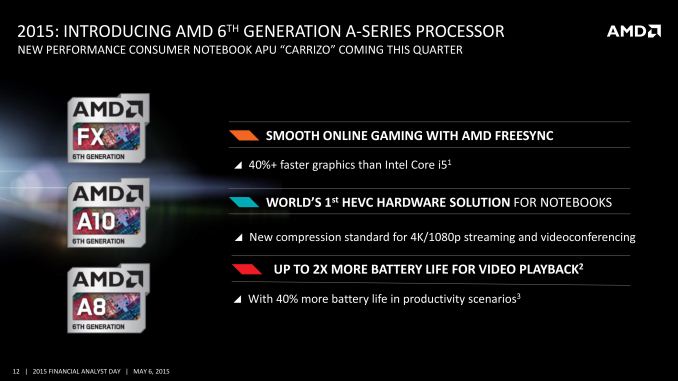
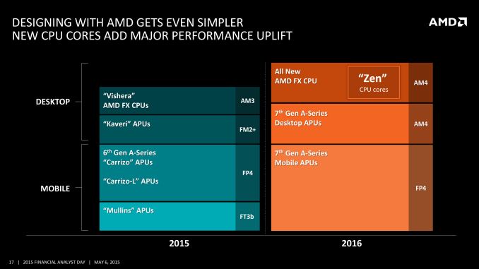
Along with AMD’s roadmap announcements today at financial analyst day, AMD has also offered a brief update on the state of Carrizo, the company’s forthcoming next-generation mobile APU. Due for launch this year, AMD has just confirmed that Carrizo is ramping well and will be launching this quarter, though SKU details are not being provided at this time.


Meanwhile, AMD is also using the opportunity to announce their intended branding for Carrizo notebooks. These products will now be known as the 6th generation A-series, and will be featuring revised AMD badges to indicate this. AMD will be retaining the current FX/A10/A8 branding, with the only real change being the inclusion of the “6th generation” branding on the badges.


Badging aside, AMD still will have to face the fact that they’re launching a 28nm notebook APU versus Intel’s 14nm notebook CPUs, the company is once again banking on their strong GPU performance to help drive sales. Coupled with the combination of low power optimizations in Carrizo and full fixed-function hardware decoding of HEVC, and AMD will be relying on Carrizo to carry them through to 2016 and Zen.


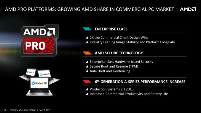
Finally, though it will come a bit later in the year, AMD’s FAD update has also briefly mentioned their plans for their AMD Pro lineup and how Carrizo will impact it. In short, AMD will be leaning on a combination of Carrizo’s power gains, and their own security technology as found in the Pro APUs.

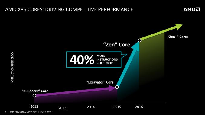
AMD Zen core leaked: Successor to Excavator core

New leaked AMD Zen slide

High performance monster
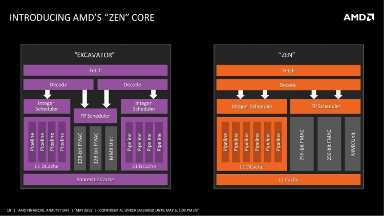
The block diagram of the new AMD Zen core has found its way onto the Planet 3 news group.
If the leak is accurate it compares the Zen, on the right, with AMD's upcoming and last Clustered Multithreading / CMT CPU core code named Excavator.
Excavator is the last of AMD's Bulldozer family of cores and it will appear with AMD's Carrizo APU, which AMD claims will be the most power efficient mainstream APU.
Zen takes a more traditional AMD CPU layout similar to Phenom. There appears to be one integer cluster in a Zen core while there are two as in the Excavator. Bulldozer had a high integer throughput at the expense of floating point performance.
In Zen AMD uses a single fetch and single decode unit on the front end which is also a step back from Steamroller's double decoders that were introduced with.
It appears then that Zen will have a higher single threaded integer and floating point performance compared to Excavator and Bulldozer.
AMD has introduced a floating point that's twice as wide as that of Excavator. Featuring two FMAC 256-bit units. These will probably fuse and process 512-bit AVX floating point instructions. In Bulldozer this is carried out by two 128-bit FMAC units. They can process one 128-bit SIMD instruction each per clock or fuse to process a single 256-bit AVX instruction per cycle. So it looks like Zen's FPU will go the same way and allow both FMACs to cooperate and process 512bit AVX instructions.
Zen enables 512bit AVX support, and with the wider floating point unit can process less complex instructions at double the rate of Excavator. Historically AMD did well with floating point performance until Bulldozer so this will be a return to form.
Zen features a 50 per cent wider integer pipeline vs a single Excavator core. Which will also dramatically improve the single threaded / per core performance of Zen.
Coupled with a more advanced 14nm process from Samsung/Globalfoundries the net result should be a significantly faster, leaner, smaller and more power efficient CPU core than Excavator.
We are expecting to see the products in the shops next year with more official information coming out in a couple of weeks.

In-detail : How Nvidia's NVLink Boosts GPU Performance

NVLink is a new feature for Nvidia GPUs that aims to drastically improve performance by increasing the total bandwidth between the GPU and other parts of the system.
In modern PCs, GPUs and numerous other devices are connected by PCI-E lanes to the CPU's or the motherboard's chipset. For some GPUs, using the available PCI-E lanes provides sufficient bandwidth that a bottleneck does not occur, but for high-end GPUs and multi-GPU setups, the number of PCI-E lanes and total bandwidth available is insufficient to meet the needs of the GPU(s) and can cause a bottleneck.

        
In an attempt to improve this situation, some motherboard manufacturers will sometimes opt to use PLX chips, which can help better utilize the bandwidth from the PCI-E lanes coming from the CPU, but overall bandwidth does not really increase. Nvidia's solution to this problem is called NVLink.
According to Nvidia, NVLink is the world's first high-speed interconnect technology for GPUs, and it allows data to be transferred between the GPU and CPU five to 12 times faster than PCI-E. Nvidia also claimed that application performance using NVLink can be up to twice as fast, relative to PCI-E.

Programs that utilize the Fast Fourier Transform (FFT) algorithm, which is heavily used in seismic processing, signal processing, image processing and partial differential equations, see the greatest performance increase. These types of applications are heavily used inside of servers and are typically bottlenecked by the PCI-E bus.
Other applications used in various fields of research see performance increases, too. According to Nvidia, one application used to study the behavior of matter by simulating molecular structures, called AMBER, gains up to a 50 percent performance increase using NVLink.


When two GPUs are utilized inside of the same system, they can be joined by four NVLink links, which can provide 20 GB/s transfer per link, totaling 80 GB/s transfer between the two cards. Because the cards no longer need to communicate using some of the scarce PCI-E bandwidth, this frees up additional bandwidth for the CPU to send data to the GPUs.
Nvidia claimed that IBM is currently integrating it into future POWER CPUs, and the U.S. Department of Energy announced that it will utilize NVLink in its next flagship supercomputer.
Source

NVIDIA Announces Tegra 4i(Project Grey)-With Integrated LTE and Phoenix Reference Design

NVIDIA Announces Tegra 4i(Project Grey)-With Integrated LTE and Phoenix Reference Design


It has been a while since we’ve heard anything about Project Grey, the first NVIDIA SoC with an integrated digital baseband, and the result of NVIDIA’s acquisition of soft-modem manufacturer Icera. Today, NVIDIA is ready to formalize Project Grey as Tegra 4i, and we have a bunch of information about this SoC and will obtain even more before MWC is upon us. NVIDIA’s roadmap from late 2011 put Grey in early 2013, and while other members of that roadmap haven’t necessarily stuck to the promised release schedule, Grey seems to be somewhere close to that schedule, at least as far as announcement and samples are concerned.
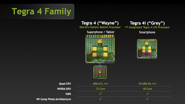


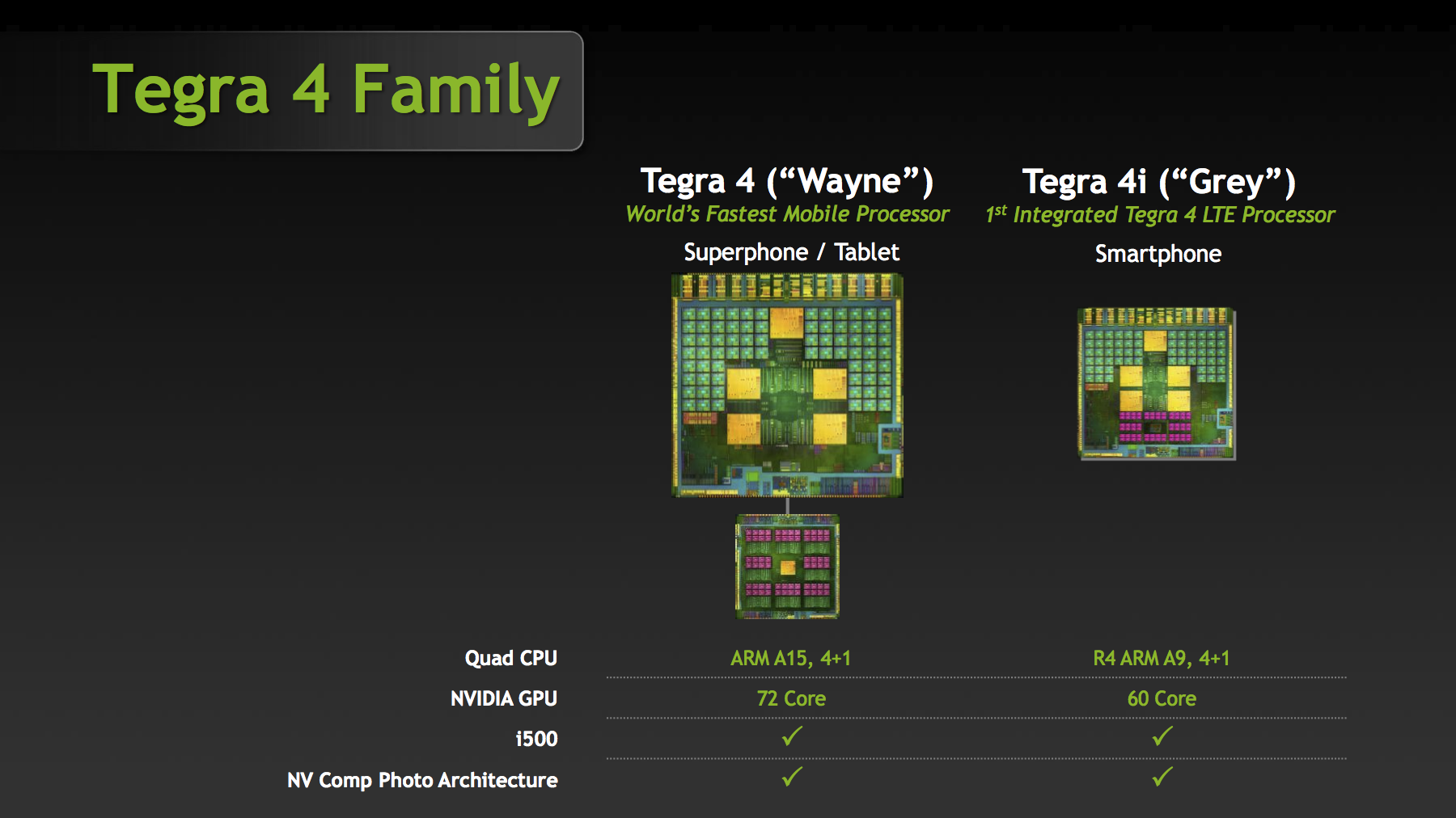
First, Tegra 4i includes the familiar 4+1 arrangement of cores we've seen since Tegra 3, but instead of Tegra 4's A15s, 4i includes ARM Cortex A9 CPUs running at a maximum single core clock of 2.3 GHz, we’re still waiting on a breakdown of the clock rates for dual and quad configuration, as well as the shadow core. NVIDIA has noted that it using R4 of ARM’s Cortex A9, which includes higher IPC thanks to the addition of a better data prefetching engine, dedicated hardware for cache preload instructions and some larger buffers. NVIDIA believes it is the first to implement the latest version of ARM's Cortex A9 core, however there's nothing stopping others from doing the same.


NVIDIA likely chose to integrate ARM's Cortex A9 r4 instead of the Cortex A15 to reduce power consumption and die size. While Tegra 4 is expected to be around 80mm^2, Tegra 4i measures in at around 60mm^2 including integrated baseband. NVIDIA isn't talking about memory interfaces at this point, but do keep in mind that your memory interface is often defined by the size of your die.
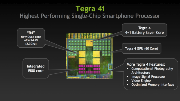


The 4i SoC is also built on TSMC’s 28 HPM process, interestingly enough not the 28 HPL process used for Tegra 4. As Tegra 4i appears to be geared towards hitting very high clock speeds, the use of TSMC's 28nm HPM process makes sense.


Tegra 4i also gets the exact same ISP and computational photography features that Tegra 4 includes, along with the same video encode and decode blocks. When it comes to the GPU side, 4i includes 60 GPU cores, that's just shy of the 72 in Tegra 4 proper. We’re waiting on additional detail to understand if these cores include the same enhancements we saw in Tegra 4 vs. Tegra 3. We also don't know the clock speed of the GPU cores in Tegra 4i.


Tegra 4 Comparison
Tegra 4Tegra 4i
CPU Configuration4+1 ARM Cortex A154+1 ARM Cortex A9 "r4"
Single CPU Max Clock1.9 GHz2.3 GHz
Process28nm HPL28nm HPM
GPU Cores7260
Memory InterfacePCDDR3 and LPDDR3LPDDR3
Display3200x20001920x1200
BasebandNo Integrated Modem

Icera i500
LTE Cat 3/Cat 4+CA TDD,FDD
100-150 Mbps DL (50 Mbps UL)
TMs 1-8
WCDMA Cat 24/6 42 Mbps
DL (5.7 Mbps UL)Cat 24/6
TD-HSPA 4.2 Mbps DL
(2.2 Mbps UL) Including TD-SCDMA


Package23x23 BGA
14x14 FCCSP
12x12 POP
12x12 FCCSP


Tegra 4i also includes the Icera i500 baseband IP block on-die, hence i for Icera. NVIDIA has disclosed some additional detail about i500 along the lines of what we’ve already written about. There’s full support for Category 3 (100 Mbps) LTE at launch, with a later upgrade to Category 4, along with support for 10 MHz + 10 MHz LTE carrier aggregation. In addition there’s support for the rest of the 3GPP suite of air interfaces, including WCDMA / HSPA+ up to 42 Mbps (Category 24), TD-SCDMA, and GSM/EDGE. i500 is also voice enabled with VoLTE support and CS-FB voice modes. NVIDIA claims that the i500 package is 7x7mm with a 6.5x6.5mm transceiver, and there are a total of 8 primary Rx ports (bands). NVIDIA also claims support for both 2x2 MIMO and 4x4 MIMO transmission modes on LTE.


Functionally Tegra 4i is more like a heavily upgraded Tegra 3 than a Tegra 4 part thanks to the Cortex A9s.  It's clear that Tegra 4i is aimed more at the smartphone market while Tegra 4 proper aims at tablets or other platforms with a higher power budget and greater performance demands.


In terms of time frame, NVIDIA expects the first Tegra 4i designs to begin shipping at the end of 2013, with most devices appearing in Q1 of 2014. It'll be interesting to see how a Cortex A9 based design holds up in Q1 2014, although the newer core and very high clock speed should do a good job of keeping the SoC feeling more modern than you'd otherwise expect.
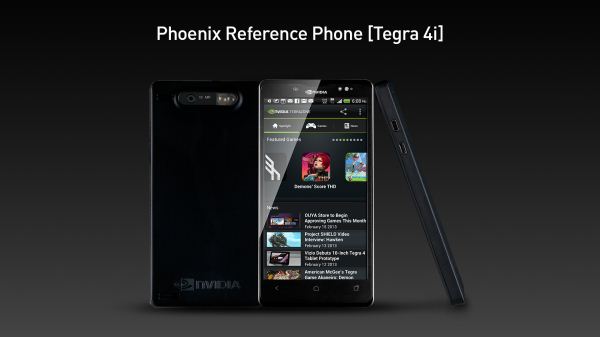


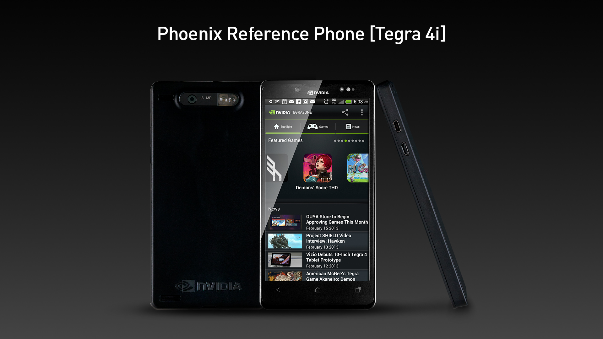
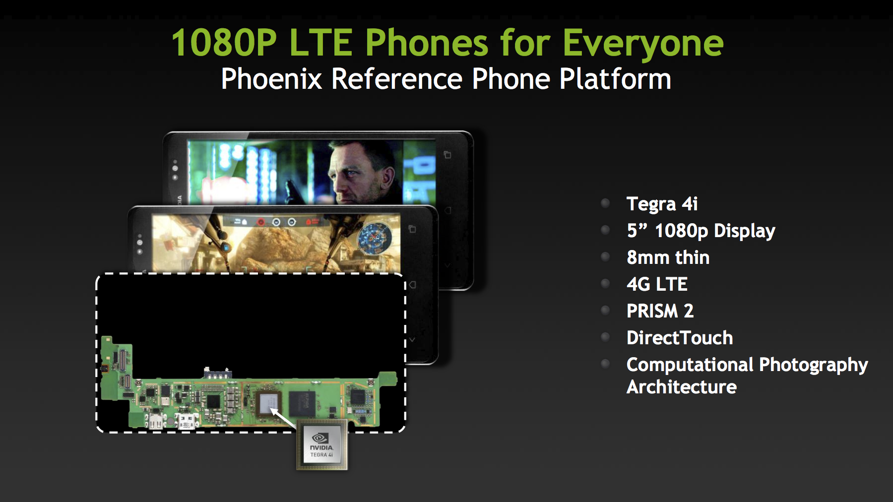
The other big announcement is a reference design built around Tegra 4i called Phoenix. It's a smartphone with Tegra 4i inside, 5-inch 1080p display, LTE, and just 8 mm of thickness. What's more impressive is that NVIDIA claims the reference design can be picked up by an OEM and ship with an unsubsidized price tag of between $100-$300 USD. With Phoenix NVIDIA now joins the likes of Qualcomm and Intel, both of whom already have active smartphone reference design programs.
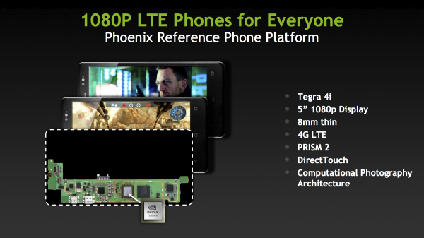


We have a lot more questions about Tegra 4, 4i, and Phoenix, but answers are coming.

Sony Announces PlayStation 4:PC-like Hardware Inside!

Sony just announced the PlayStation 4, along with some high level system specifications. The high level specs are what we've heard for quite some time:


  • 8-core x86-64 CPU using AMD Jaguar cores (built by AMD)

  • High-end PC GPU (also built by AMD), delivering 1.84TFLOPS of performance

  • Unified 8GB of GDDR5 memory for use by both the CPU and GPU with 176GB/s of memory bandwidth

  • Large local hard drive


Sony has confirmed the actual performance of the PlayStation 4's GPU as 1.84 TFLOPS. Sony claims the GPU features 18 compute units, which if this is GCN based we'd be looking at 1152 SPs and 72 texture units. It's unclear how custom the GPU is however, so we'll have to wait for additional information to really know for sure. The highest end PC GPUs are already faster than this, but the PS4's GPU is a lot faster than the PS3's RSX which was derived from NVIDIA's G70 architecture (used in the GeForce 7800 GTX, for example). I'm quite pleased with the promised level of GPU performance with the PS4. There are obvious power and cost constraints that would keep AMD/Sony from going even higher here, but this should be a good leap forward from current gen consoles.


Outfitting the PS4 with 8GB of RAM will be great for developers, and using high-speed GDDR5 will help ensure the GPU isn't bandwidth starved. Sony promised around 176GB/s of memory bandwidth for the PS4. The lack of solid state storage isn't surprising. Hard drives still offer a dramatic advantage in cost per GB vs. an SSD. Now if it's user replaceable with an SSD that would be a nice compromise.


Backwards compatibility with PS3 games isn't guaranteed and instead will leverage cloud gaming to stream older content to the box. There's some sort of a dedicated background processor that handles uploads and downloads, and even handles updates in the background while the system is off. The PS4 also supports instant suspend/resume.


The most intriuging thing is that the actual console has not been shown,only the internal details,controllers and how it works..

Qualcomm Snapdragon 200,400 processors detailed


Qualcomm Snapdragon 200, 400 processors detailed


new snapdragon chip Qualcomm Snapdragon 200, 400 processors detailedQualcomm has posted the details pertaining to new SoCs for entry and mid-range smartphones/tablets today. Dubbed as Snapdragon 200 and Snapdragon 400, these processors will be seen in several Android devices later this year.


According to Qualcomm, Snapdragon 200 processors include quad ARM Cortex-A5 CPUs up to 1.4GHz per core, along with Adreno 203 GPU. These SoCs support HD video playback, CDMA multimode/UMTS modem options, dual-sim dual standby and upto 8 megapixels camera.


On the other hand, Snapdragon 400 processors will come in two variants, one with Dual Krait CPUs running at up to 1.7GHz per core and other with Quad ARM Cortex A7 CPUs running at up to 1.4GHz per core. Both the variants will have Adreno 305 GPU. The chips support Miracast wireless display technology, upto 13.5MP cameras, premium audio, and 1080p video capture, playback and almost all modem technologies.


“Earlier this year, Qualcomm announced the new tiering structure for Snapdragon processors, including Snapdragon 800, 600, 400 and 200. While the Snapdragon 800 and 600 processors are clearly targeted at premier and high end smartphones, tablets and mobile computing devices, the Snapdragon 400 and Snapdragon 200 processors take Qualcomm’s technology leadership into the mid-tier and entry level smartphone segments,” Tim McDonough, Vice President, Marketing, Qualcomm Mobile & Computing noted in a blog post


3GHz NovaThor L8580 CPU to debut on MWC 2013 floors

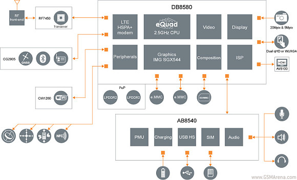
ST-Ericsson unveiled their latest 2.5GHz NovaThor L8580 CPU earlier in this year, but the company is now readying to showcase an even faster version of the chip at MWC 2013.


The four Cortex A9 cores residing in the NovaThor L8580 (or eQuad, as it's also dubbed) that's going to be on display at MWC are going to be clocked at 3GHz. In order to not drain the battery in a heartbeat, ST-Ericsson have build the chipset using the 28nm FD-SOI manufacturing technology.


The company has also utilized ModAp, which optimizes the execution of apps and as a result runs them up to 35% faster. The chip comes with support for dual cameras (of up to 20MP), HD Voice and LTE. The GPU is going to be of the PowerVR SGX544 variety clocked at 600MHz.


Naturally, the 3GHz NovaThor L8580 CPU in question is just a prototype at the moment, but hopefully, we'll get to play with it in Barcelona and put it through some benchmarking.